デモカタログ / モータードライバー
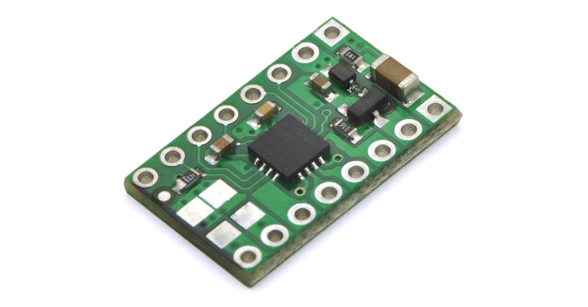
DRV8833 dual motor driver carrier
Pololu · MPN 2130 · エージェント向け表示
$10.95参考値 · 2026-08-22
表示の日付時点で Pololu 自身の構造化データから取得したものです — 見積りではありません。在庫の有無は意図的に示していません。
| Pololu | $10.95 · 2026-08-22 | 製品ページ ↗ |
Partsgraph 裏付け済み仕様書(PDF)自社作成 · 以下の出典から編集
TI DRV8833 datasheetsha256 3e400e333f08…
仕様 — すべての値に根拠が付いています
電気特性
| RMS 出力電流 / ブリッジ(IC 規定値) | 1.5 A | データシート p.1“The output driver block of each H-bridge consists of – 1.5-A RMS, 2-A Peak per H-Bridge in PWP N”https://www.ti.com/lit/ds/symlink/drv8833.pdfsha256 3e400e333f08… |
| 電流チョッピングの基準電圧 | 200 mV | データシート p.10“with a reference voltage. The reference voltage is fixed at 200 mV. The chopping current is calculated in Equation 1.”https://www.ti.com/lit/ds/symlink/drv8833.pdfsha256 3e400e333f08… |
| 低消費電力スリープモード | はい | データシート p.1“overtemperature. A low-power sleep mode is also • Wide Power Supply Voltage Range:”https://www.ti.com/lit/ds/symlink/drv8833.pdfsha256 3e400e333f08… |
| 並列接続時の連続電流 | 2.4 A | ベンダーページ“peak) per motor Motor outputs can be paralleled to deliver 2.4 A continuous (4 A peak) to a single motor Inputs are 3V- and” |
| 並列接続時のピーク電流 | 4 A | ベンダーページ“otor outputs can be paralleled to deliver 2.4 A continuous (4 A peak) to a single motor Inputs are 3V- and 5V-compatible Un” |
| 逆電圧保護 | はい | ベンダーページ“ut and protection against over-current and over-temperature Reverse-voltage protection circuit Current limiting can be enabled by adding sense res” |
| 低電圧ロックアウト | はい | ベンダーページ“A peak) to a single motor Inputs are 3V- and 5V-compatible Under-voltage lockout and protection against over-current and over-temperature Re” |
| VM 絶対最大 (V) | 11.8 | データシート p.5“–0.3 11.8 V Digital input pin volta”https://www.ti.com/lit/ds/symlink/drv8833.pdfsha256 3e400e333f08… |
| デジタル入力電圧、推奨 max (V) | 5.75 | データシート p.5“–0.3 5.75 V IOUT RTY package continuous RMS or DC output”https://www.ti.com/lit/ds/symlink/drv8833.pdfsha256 3e400e333f08… |
| MOSFET のオン抵抗、HS + LS (mΩ) | 360 | データシート p.1“ons. Motor – Low MOSFET ON-Resistance: HS + LS 360 The device has two H-bridge drive”https://www.ti.com/lit/ds/symlink/drv8833.pdfsha256 3e400e333f08… |
| スリープモードの電源電流、typ @ VM=5V (μA) | 1.6 | データシート p.6“VM = 5 V 1.6 2.5 μA VUVLO VM undervoltage lockou”https://www.ti.com/lit/ds/symlink/drv8833.pdfsha256 3e400e333f08… |
| UVLO しきい値、VM 下降時 max (V) | 2.6 | データシート p.6“2.6 V VM undervoltage lockout VHYS”https://www.ti.com/lit/ds/symlink/drv8833.pdfsha256 3e400e333f08… |
| 入力プルダウン、nSLEEP (kΩ) | 500 | データシート p.6“nSLEEP 500 RPD Input pulldown resistance”https://www.ti.com/lit/ds/symlink/drv8833.pdfsha256 3e400e333f08… |
| 過電流保護の動作値、typ (A) | 3.3 | データシート p.6“2 3.3 A tDEG OCP Deglitch time”https://www.ti.com/lit/ds/symlink/drv8833.pdfsha256 3e400e333f08… |
| 熱シャットダウン温度、typ (°C) | 160 | データシート p.6“Die temperature 150 160 180 °C (1) Internal dead time. External”https://www.ti.com/lit/ds/symlink/drv8833.pdfsha256 3e400e333f08… |
性能
| 電流制御の PWM 周波数、typ (kHz) | 50 | データシート p.6“nternal PWM frequency 50 kHz tR Rise time”https://www.ti.com/lit/ds/symlink/drv8833.pdfsha256 3e400e333f08… |
| INx から OUTx への伝搬遅延、typ (µs) | 1.1 | データシート p.6“VM = 5 V 1.1 µs tDEAD Dead time (1)”https://www.ti.com/lit/ds/symlink/drv8833.pdfsha256 3e400e333f08… |
| 電流検出のブランキング時間 | 3.75 μs | データシート p.10“the current sense circuitry. This blanking time is fixed at 3.75 μs. This blanking time also sets the minimum on time of the PW”https://www.ti.com/lit/ds/symlink/drv8833.pdfsha256 3e400e333f08… |
インターフェース
| ロジック入力の互換性 | 3V- and 5V-compatible | ベンダーページ“er 2.4 A continuous (4 A peak) to a single motor Inputs are 3V- and 5V-compatible Under-voltage lockout and protection against over-current a” |
| バイポーラステッピングモーターを 1 台駆動可能 | one bipolar stepper motor | ベンダーページ“ures Dual-H-bridge motor driver: can drive two DC motors or one bipolar stepper motor Operating voltage: 2.7 V to 10.8 V Output current: 1.2 A” |
| nSLEEP は基板上でプルアップ(既定で有効) | はい | ベンダーページ“ontrol connections are made on the other. The nSLEEP pin is pulled high on the board and can be left disconnected if you do not want to use the” |
| nFAULT オープンドレイン出力(外部プルアップが必要) | はい | ベンダーページ“the inputs affect the driver outputs. The nFAULT pin is an open-drain output that is driven low by the chip whenever an over-current, ov” |
機構
| ドライバー IC のパッケージ | 16-pin WQFN | データシート p.1“The DRV8833 is packaged in a 16-pin WQFN • PWM Winding Current Regulation and Current”https://www.ti.com/lit/ds/symlink/drv8833.pdfsha256 3e400e333f08… |
| 電流検出パッドは 1206 抵抗に対応した寸法 | 1206 | ベンダーページ“nt, as indicated in the image below. The pads are sized for 1206 surface-mount resistors. Refer to the DRV8833 datasheet for” |
| 付属ヘッダー | 1x8-pin breakaway 0.1″ male headers | ベンダーページ“and other components connected to it. Included hardware Two 1x8-pin breakaway 0.1″ male headers are included with the DRV8833 dual motor driver carrier, wh” |
法規適合
| RoHS | RoHS | データシート p.1“package with PowerPAD™ (Eco-friendly: RoHS & no Limiting”https://www.ti.com/lit/ds/symlink/drv8833.pdfsha256 3e400e333f08… |
| ESD 耐量、HBM (V) | ±4000 | データシート p.5“er ANSI/ESDA/JEDEC JS-001, all pins (1) ±4000 Electrostatic V(ESD)”https://www.ti.com/lit/ds/symlink/drv8833.pdfsha256 3e400e333f08… |
一般
| チャンネル数 | dual | ベンダーページ“pat qty  Save This tiny breakout board for TI’s DRV8833 dual motor driver can deliver 1.2 A per channel continuously (2” |
| モーター電源範囲 | 2.7 〜 10.8 V | データシート p.1“tage Range: provided. 2.7 to 10.8 V”https://www.ti.com/lit/ds/symlink/drv8833.pdfsha256 3e400e333f08… |
| ピーク出力電流 / チャンネル | 2 A | データシート p.1“driver block of each H-bridge consists of – 1.5-A RMS, 2-A Peak per H-Bridge in PWP N-channel”https://www.ti.com/lit/ds/symlink/drv8833.pdfsha256 3e400e333f08… |
| 連続出力電流 / チャンネル | 1.2 A | ベンダーページ“eakout board for TI’s DRV8833 dual motor driver can deliver 1.2 A per channel continuously (2 A peak) to a pair of DC motors.” |
使用しているビルド
2WD 探索ロボット — 役割: モータードライバー